- 您现在的位置:买卖IC网 > Sheet目录1214 > EVAL-ADE7763ZEB (Analog Devices Inc)BOARD EVALUATION FOR ADE7763
�� ��
��
��Data� Sheet�
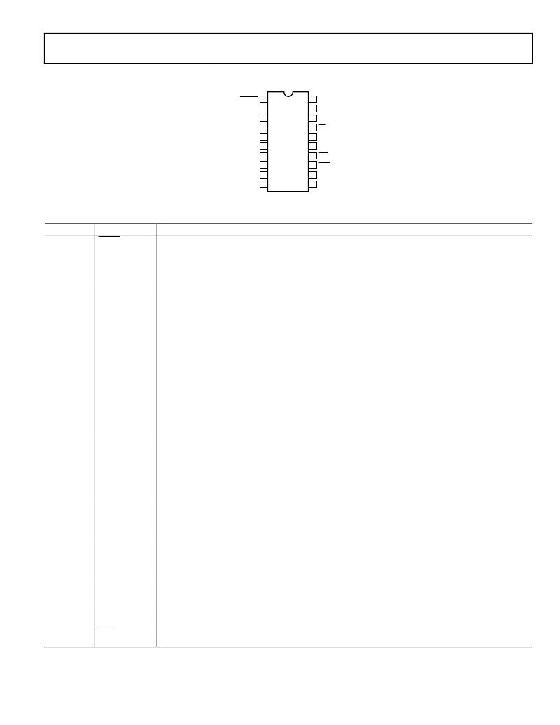
�PIN� CONFIGURATION� AND� FUNCTION� DESCRIPTIONS�
�ADE7763�
�RESET� 1�
�DVDD� 2�
�AVDD� 3�
�20�
�19�
�18�
�DIN�
�DOUT�
�SCLK�
�V1P� 4�
�V1N� 5�
�ADE7763�
�TOP� VIEW�
�17� CS�
�16� CLKOUT�
�V2N� 6� (Not� to� Scale)� 15� CLKIN�
�V2P� 7�
�AGND� 8�
�REF� IN/OUT� 9�
�DGND� 10�
�14�
�13�
�12�
�11�
�IRQ�
�SAG�
�ZX�
�CF�
�Figure� 5.� Pin� Configuration� (SSOP� Package)�
�Table� 4.� Pin� Function� Descriptions�
�Pin� No.�
�1�
�2�
�3�
�4,� 5�
�6,� 7�
�8�
�9�
�10�
�11�
�12�
�13�
�Mnemonic�
�RESET�
�DVDD�
�AVDD�
�V1P,� V1N�
�V2N,� V2P�
�AGND�
�REF� IN/OUT�
�DGND�
�CF�
�ZX�
�SAG�
�Description�
�Reset� Pin� 1� .� A� logic� low� on� this� pin� holds� the� ADCs� and� digital� circuitry� (including� the� serial� interface)� in� a�
�reset� condition.�
�Digital� Power� Supply.� This� pin� provides� the� supply� voltage� for� the� digital� circuitry.� The� supply� voltage�
�should� be� maintained� at� 5� V� ±� 5%� for� specified� operation.� This� pin� should� be� decoupled� to� DGND� with� a�
�10� μF� capacitor� in� parallel� with� a� ceramic� 100� nF� capacitor.�
�Analog� Power� Supply.� This� pin� provides� the� supply� voltage� for� the� analog� circuitry.� The� supply� should� be�
�maintained� at� 5� V� ±� 5%� for� specified� operation.� Minimize� power� supply� ripple� and� noise� at� this� pin� by� using�
�proper� decoupling.� The� typical� performance� graphs� show� the� power� supply� rejection� performance.� This�
�pin� should� be� decoupled� to� AGND� with� a� 10� μF� capacitor� in� parallel� with� a� ceramic� 100� nF� capacitor.�
�Analog� Inputs� for� Channel� 1.� This� channel� is� intended� for� use� with� a� di/dt� current� transducer,� i.e.,� a�
�Rogowski� coil� or� another� current� sensor� such� as� a� shunt� or� current� transformer� (CT).� These� inputs� are� fully�
�differential� voltage� inputs� with� maximum� differential� input� signal� levels� of� ±0.5� V,� ±0.25� V,� and� ±0.125� V,�
�depending� on� the� full-scale� selection—see� the� Analog� Inputs� section.� Channel� 1� also� has� a� PGA� with� gain�
�selections� of� 1,� 2,� 4,� 8,� or� 16.� The� maximum� signal� level� at� these� pins� with� respect� to� AGND� is� ±0.5� V.� Both�
�inputs� have� internal� ESD� protection� circuitry� and� can� sustain� an� overvoltage� of� ±6� V� without� risk� of�
�permanent� damage.�
�Analog� Inputs� for� Channel� 2.� This� channel� is� intended� for� use� with� the� voltage� transducer.� These� inputs� are�
�fully� differential� voltage� inputs� with� a� maximum� differential� signal� level� of� ±0.5� V.� Channel� 2� also� has� a� PGA�
�with� gain� selections� of� 1,� 2,� 4,� 8,� or� 16.� The� maximum� signal� level� at� these� pins� with� respect� to� AGND� is�
�±0.5� V.� Both� inputs� have� internal� ESD� protection� circuitry� and� can� sustain� an� overvoltage� of� ±6� V� without�
�risk� of� permanent� damage.�
�Analog� Ground� Reference.� This� pin� provides� the� ground� reference� for� the� analog� circuitry,� i.e.,� ADCs� and�
�reference.� This� pin� should� be� tied� to� the� analog� ground� plane� or� to� the� quietest� ground� reference� in� the�
�system.� Use� this� quiet� ground� reference� for� all� analog� circuitry,� such� as� antialiasing� filters� and� current� and�
�voltage� transducers.� To� minimize� ground� noise� around� the� ADE7763,� connect� the� quiet� ground� plane�
�to� the� digital� ground� plane� at� only� one� point.� It� is� acceptable� to� place� the� entire� device� on� the� analog�
�ground� plane.�
�Access� to� the� On-Chip� Voltage� Reference.� The� on-chip� reference� has� a� nominal� value� of� 2.4� V� ±� 8%� and� a�
�typical� temperature� coefficient� of� 30� ppm/°C.� An� external� reference� source� can� also� be� connected� at� this�
�pin.� In� either� case,� this� pin� should� be� decoupled� to� AGND� with� a� 10� μF� capacitor� in� parallel� with� a� 100nF�
�ceramic� capacitor.�
�Digital� Ground� Reference.� This� pin� provides� the� ground� reference� for� the� digital� circuitry,� i.e.,� multiplier,�
�filters,� and� digital-to-frequency� converter.� Because� the� digital� return� currents� in� the� ADE7763� are� small,� it� is�
�acceptable� to� connect� this� pin� to� the� analog� ground� plane� of� the� system.� However,� high� bus� capacitance�
�on� the� DOUT� pin� could� result� in� noisy� digital� current,� which� could� affect� performance.�
�Calibration� Frequency� Logic� Output.� The� CF� logic� output� gives� active� power� information.� This� output� is�
�intended� to� be� used� for� operational� and� calibration� purposes.� The� full-scale� output� frequency� can� be�
�adjusted� by� writing� to� the� CFDEN� and� CFNUM� registers—see� the� Energy-to-Frequency� Conversion� section.�
�Voltage� Waveform� (Channel� 2)� Zero-Crossing� Output.� This� output� toggles� logic� high� and� logic� low� at� the�
�zero� crossing� of� the� differential� signal� on� Channel� 2—see� the� Zero-Crossing� Detection� section.�
�This� open-drain� logic� output� goes� active� low� when� either� no� zero� crossings� are� detected� or� a� low� voltage�
�threshold� (Channel� 2)� is� crossed� for� a� specified� duration—see� the� Line� Voltage� Sag� Detection� section.�
�Rev.� C� |� Page� 9� of� 56�
�发布紧急采购,3分钟左右您将得到回复。
相关PDF资料
EVAL-ADE7816EBZ
BOARD EVALUATION FOR ADE7816
EVAL-ADE7878EBZ
BOARD EVAL FOR ADE7878
EVAL-ADE7880EBZ
BOARD EVAL FOR ADE7880
EVAL-ADE7953EBZ
BOARD EVAL FOR ADE7953
EVAL-ADF4002EBZ1
BOARD EVAL FOR ADF4002
EVAL-ADG788EBZ
BOARD EVALUATION FOR ADG788
EVAL-ADM1021AEB
BOARD EVAL FOR ADM1021
EVAL-ADM1023EB
BOARD EVAL FOR ADM1023
相关代理商/技术参数
EVAL-ADE7816EBZ
功能描述:BOARD EVALUATION FOR ADE7816 RoHS:是 类别:编程器,开发系统 >> 评估演示板和套件 系列:- 标准包装:1 系列:PSoC® 主要目的:电源管理,热管理 嵌入式:- 已用 IC / 零件:- 主要属性:- 次要属性:- 已供物品:板,CD,电源
EVAL-ADE7854EBZ
制造商:Analog Devices 功能描述:EVALUATION BOARDS - Boxed Product (Development Kits)
EVAL-ADE7858EBZ
制造商:AD 制造商全称:Analog Devices 功能描述:Poly Phase Multifunction Energy Metering IC with per Phase Active and Reactive Powers
EVAL-ADE7878EBZ
功能描述:BOARD EVAL FOR ADE7878 RoHS:是 类别:编程器,开发系统 >> 评估演示板和套件 系列:- 标准包装:1 系列:PCI Express® (PCIe) 主要目的:接口,收发器,PCI Express 嵌入式:- 已用 IC / 零件:DS80PCI800 主要属性:- 次要属性:- 已供物品:板
EVAL-ADE7880EBZ
功能描述:BOARD EVAL FOR ADE7880 RoHS:是 类别:编程器,开发系统 >> 评估演示板和套件 系列:* 产品培训模块:Obsolescence Mitigation Program 标准包装:1 系列:- 主要目的:电源管理,电池充电器 嵌入式:否 已用 IC / 零件:MAX8903A 主要属性:1 芯锂离子电池 次要属性:状态 LED 已供物品:板
EVAL-ADE7880EBZ
制造商:Analog Devices 功能描述:ADE7880, ENERGY METER, 3 PH, SPI, I2C, E
EVAL-ADE7913EBZ
制造商:AD 制造商全称:Analog Devices 功能描述:3-Channel, Isolated, Sigma-Delta ADC with SPI
EVAL-ADE7953EBZ
功能描述:BOARD EVAL FOR ADE7953 RoHS:是 类别:编程器,开发系统 >> 评估演示板和套件 系列:- 标准包装:1 系列:PSoC® 主要目的:电源管理,热管理 嵌入式:- 已用 IC / 零件:- 主要属性:- 次要属性:- 已供物品:板,CD,电源